Difference between revisions of "8-bit-level-shifter"
From SB-Components Wiki
| (8 intermediate revisions by the same user not shown) | |||
| Line 25: | Line 25: | ||
</div> | </div> | ||
<div class="large-4 column"> | <div class="large-4 column"> | ||
| − | [[File: | + | [[File:8-bit_level_shifter.png|thumb|left|alt=8 bit level shifter| Buy it From : ''[https://shop.sb-components.co.uk/products/8-bit-level-shifter Click Here]'']] |
</div> | </div> | ||
</div> | </div> | ||
| Line 34: | Line 34: | ||
<tr> <th> Pinout </th> <th> Description </th></tr> | <tr> <th> Pinout </th> <th> Description </th></tr> | ||
| − | <tr> <td> VA </td> <td> A-port supply voltage. 1. | + | <tr> <td> VA </td> <td> A-port supply voltage. 1.2 V ≤ VA ≤ 3.6 V, VA ≤ VB </td></tr> |
<tr> <td> VB </td> <td> B-port supply voltage. 1.65 V ≤ VB ≤ 5.5 V </td></tr> | <tr> <td> VB </td> <td> B-port supply voltage. 1.65 V ≤ VB ≤ 5.5 V </td></tr> | ||
<tr> <td> OE </td> <td> Output enable, by default set to high </td></tr> | <tr> <td> OE </td> <td> Output enable, by default set to high </td></tr> | ||
| Line 43: | Line 43: | ||
== Installation == | == Installation == | ||
| + | The 8-bit level shifter breakout device has two functional modes, enabled and disabled. To disable the device, set the '''OE input''' | ||
| + | low (By default set to High using '''resistor R2'''), which places all I/Os in a high impedance state. Setting the OE input high will enable the device. | ||
| + | |||
==== Block Diagram ==== | ==== Block Diagram ==== | ||
* Typical Application Block Diagram for TXB0108 | * Typical Application Block Diagram for TXB0108 | ||
| Line 48: | Line 51: | ||
==== Reference Circuit ==== | ==== Reference Circuit ==== | ||
| − | [[File:8bit_level_shifter_ref_ckt.jpg]] | + | [[File:8bit_level_shifter_ref_ckt.jpg| 600px]] |
== Resources == | == Resources == | ||
Latest revision as of 05:54, 24 June 2021
8 Bit Level Shifter Breakout
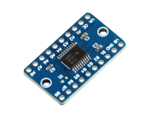
The 8-bit level shifter is an 8-bit non-inverting shifter breakout board with the powerful and compact IC TXB0108 and VCCA Voltage Range: 1.2V-3.6V and VCCB Voltage Range: 1.65V-5.5V that acts as a bridge between applications with differing source voltage and input-output voltage levels.
Features
- VCC Isolation Feature – If Either VCC Input Is at GND, All Outputs Are in the High-Impedance State
- Low power consumption
- High conversion speed, up to 60Mbps in push-pull applications, up to 2Mbps in open-drain applications
- Bidirectional automatic conversion, no direction control needed
- OE Input Circuit Referenced to VCCA
- Ioff Supports Partial-Power-Down Mode Operation
Specifications
- VCCA Voltage Range: 1.2V-3.6V
- VCCB Voltage Range: 1.65V-5.5V
- Conditions of Use: VCCB>VCCA
- Working Current: 30uA
- Support Port: push-pull, open-drain
- Conversion Speed: push-pull 60Mbps(MAX)\open-drain 2Mbps(MAX)
- Working Temperature Range: -30℃~75℃
- IC - TXB0108
- Power Consumption - 4μA Max ICC

Buy it From : Click Here
Pinout
| Pinout | Description |
|---|---|
| VA | A-port supply voltage. 1.2 V ≤ VA ≤ 3.6 V, VA ≤ VB |
| VB | B-port supply voltage. 1.65 V ≤ VB ≤ 5.5 V |
| OE | Output enable, by default set to high |
| GND | Ground |
| A1-A8 | Input/Output 1-8, Referenced to VA |
| B1-B8 | Input/Output 1-8, Referenced to VB |
Installation
The 8-bit level shifter breakout device has two functional modes, enabled and disabled. To disable the device, set the OE input low (By default set to High using resistor R2), which places all I/Os in a high impedance state. Setting the OE input high will enable the device.
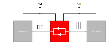
Block Diagram
- Typical Application Block Diagram for TXB0108


