Difference between revisions of "8-bit-level-shifter"
From SB-Components Wiki
| Line 48: | Line 48: | ||
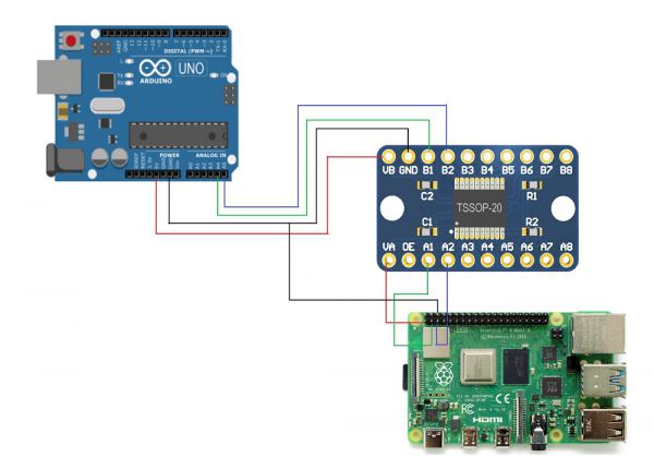
==== Reference Circuit ==== | ==== Reference Circuit ==== | ||
| − | [[File:8bit_level_shifter_ref_ckt.jpg]] | + | [[File:8bit_level_shifter_ref_ckt.jpg| 600px]] |
== Resources == | == Resources == | ||
Revision as of 10:05, 17 June 2021
8 Bit Level Shifter Breakout
The 8-bit level shifter is an 8-bit non-inverting shifter breakout board with the powerful and compact IC TXB0108 and VCCA Voltage Range: 1.2V-3.6V and VCCB Voltage Range: 1.65V-5.5V that acts as a bridge between applications with differing source voltage and input-output voltage levels.
Features
- VCC Isolation Feature – If Either VCC Input Is at GND, All Outputs Are in the High-Impedance State
- Low power consumption
- High conversion speed, up to 60Mbps in push-pull applications, up to 2Mbps in open-drain applications
- Bidirectional automatic conversion, no direction control needed
- OE Input Circuit Referenced to VCCA
- Ioff Supports Partial-Power-Down Mode Operation
Specifications
- VCCA Voltage Range: 1.2V-3.6V
- VCCB Voltage Range: 1.65V-5.5V
- Conditions of Use: VCCB>VCCA
- Working Current: 30uA
- Support Port: push-pull, open-drain
- Conversion Speed: push-pull 60Mbps(MAX)\open-drain 2Mbps(MAX)
- Working Temperature Range: -30℃~75℃
- IC - TXB0108
- Power Consumption - 4μA Max ICC
File:8bit level shifter.png
Buy it From : Click Here
Pinout
| Pinout | Description |
|---|---|
| VA | A-port supply voltage. 1.1 V ≤ VA ≤ 3.6 V, VA ≤ VB |
| VB | B-port supply voltage. 1.65 V ≤ VB ≤ 5.5 V |
| OE | Output enable, by default set to high |
| GND | Ground |
| A1-A8 | Input/Output 1-8, Referenced to VA |
| B1-B8 | Input/Output 1-8, Referenced to VB |
Installation
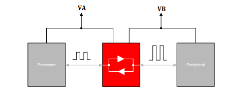
Block Diagram
- Typical Application Block Diagram for TXB0108


