Difference between revisions of "Differential-pressure-breakout"
From SB-Components Wiki
(Created page with "<div class="row"> <div class="large-8 column"> == 8 Bit Level Shifter Breakout == Differential Pressure Breakout comprises NXP's MPXV5010DP, is an Integrated Silicon Pressur...") |
(→Pinout) |
||
| Line 28: | Line 28: | ||
<tr> <th> Pinout </th> <th> Description </th></tr> | <tr> <th> Pinout </th> <th> Description </th></tr> | ||
| − | <tr> <td> | + | <tr> <td> VCC </td> <td> Positive Supply Voltage pin (5V) </td></tr> |
| − | <tr> <td> | + | <tr> <td> CS </td> <td> Chip Select Digital Input pin </td></tr> |
| − | <tr> <td> | + | <tr> <td> SCK </td> <td> Serial Clock Digital Input pin </td></tr> |
| − | <tr> <td> | + | <tr> <td> MISO </td> <td> Data/Ready Digital Output pin </td></tr> |
| − | <tr> <td> | + | <tr> <td> VOUT </td> <td> Analog Output </td></tr> |
| − | <tr> <td> | + | <tr> <td> GND </td> <td> Ground pin </td></tr> |
</table> | </table> | ||
Revision as of 06:04, 24 June 2021
8 Bit Level Shifter Breakout
Differential Pressure Breakout comprises NXP's MPXV5010DP, is an Integrated Silicon Pressure Sensor On-Chip Signal Conditioned, Temperature Compensated, and Calibrated. Differential Pressure Breakout consists of two axial ports to accommodate industrial grade tubing. In the temperature range between 0º and 85ºC, the maximum error rate of the sensor is 5.0%.
Features
- MPXV5010DP has an analog output
- Temperature Compensated over -40 to +125C
- The signal passes through the onboard 22-bit ADC before being outputted through the SPI interface
- Durable Epoxy Unibody and Thermoplastic (PPS) Surface Mount Package.
Specifications
- Operating Pressure - 1.45 psi
- Port Type - Dual Radial Barbed
- Port Size - 4.93 mm
- Interface- SPI / Analog Interface
- Measurement range- 0 to 10 kPa
File:Diff pressure breakout.png
Buy it From : Click Here
Pinout
| Pinout | Description |
|---|---|
| VCC | Positive Supply Voltage pin (5V) |
| CS | Chip Select Digital Input pin |
| SCK | Serial Clock Digital Input pin |
| MISO | Data/Ready Digital Output pin |
| VOUT | Analog Output |
| GND | Ground pin |
Installation
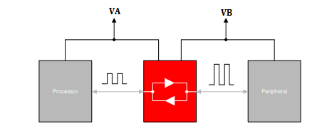
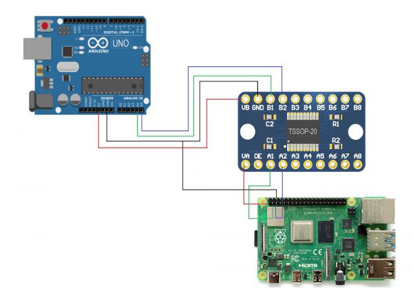
The 8-bit level shifter breakout device has two functional modes, enabled and disabled. To disable the device, set the OE input low (By default set to High using resistor R2), which places all I/Os in a high impedance state. Setting the OE input high will enable the device.
Block Diagram
- Typical Application Block Diagram for TXB0108


